PD1550A System Calibration & Compensation
Introduction to PD1550A Calibration
Oscilloscope probe compensation, calibration (AutoCal), and the shunt de-embedding file are steps that the Double-Pulse Test (DPT) system operator should perform periodically to achieve the most accurate measurements. System Calibration is a formal calibration procedure. For accurate DPT measurements, it is very important to calibrate the DPT system to insure that all delays are equivalent.
Additionally, a Full Calibration (also known as Service Calibration) is required annually for the MXR108A oscilloscope, 33512B Waveform Generator, B2902A/B Precision Source/Measure Unit, and Heinzinger EVO Power Supply test instruments.
Calibration Steps:
Set/Verify AC Line Frequency and Date/Time on the B2902A/B
1. Oscilloscope Probe Offset Compensation
Gate Resistor Module Schematic
2. Low-Side Gate Voltage Source Calibration -- VGS,L Output
3. Low-Side Common Resistor Calibration -- RCOM,L
4. Low-Side Gate Resistance Calibration -- RGON,L
5. Low-Side Gate Resistance Calibration -- RGOFF,L
6. High-Side Gate Voltage Source Calibration -- VGS,H Output
7. High-Side Common Resistor Calibration -- RCOM,H
8. High-Side Gate Resistance Calibration -- RGON,H
9. High-Side Gate Resistance Calibration -- RGOFF,H
Coaxial Shunt Resistor Characterization
Set/Verify AC Line Frequency and Date/Time on the B2902A/B
Click here for instructions
The Keysight B2902A/B Source Measure Unit (SMU) is used only for both the S-Parameter measurements and the PD1500A system calibration. Its factory default line frequency is set to 50 Hz and must be changed to 60 Hz in those countries with a 60 Hz line frequency. To change the line frequency from the instrument front panel, press the following keys:
- For setting to 50 Hz: More > System > PLC > 50 Hz
- For setting to 60 Hz: More > System > PLC > 60 Hz
Optionally, to set the Date and Time press the following:
System > Info > Date/Time
Oscilloscope Probe Compensation
Prior to running system calibration or DPT tests, the oscilloscope probes must be adjusted for low frequency compensation. The passive probes have built-in compensation RC divider networks. The differential probes also require offset compensation.
 Top
TopInitiate Calibration & Compensation Procedures
From the PD1000A Control Software, select the Double-Pulse Test Control tab. From the Settings drop-down menu, select Calibration & Compensation. Be careful to follow all instructions.
The software reads the EEPROMS on the Gate Drive and Gate Drive Resistor Modules.
1. Oscilloscope Probe Offset Compensation
As the first step calibrating the Double-Pulse Test system, the oscilloscope probes must be adjusted for low frequency compensation. For this, the N2873A passive probes have built-in compensation RC divider networks. The Keysight N2873A probe is used only with the True-Pulse Probing Unit.
Allow the oscilloscope and probe to warm up at ambient temperature for a minimum of 60 minutes (1 hour) before performing the adjustment.Required Equipment
Spring hook and ground clips for passive oscilloscope probes.
Low Frequency Compensation trimmer/adjustment tools (small non-metallic screwdriver).
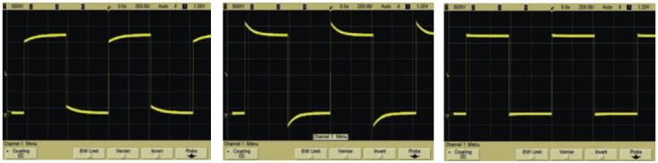
Low Frequency Compensation for the N2873A Probe
The Infiniium S-Series Oscilloscopes have a square wave reference signal available on the front panel to use for compensating the passive probes. Attach the spring hook and ground clip to the probe and then the square wave reference terminal.
- Refer to the N2873A Probe’s User Guide for instructions. A general description and procedure can also be found on page 5 (Hint #3) of the Keysight 8 Hints for Better Scope Probing.
- Connect the probe to the oscilloscope’s front-panel calibration output (a square wave label is seen near this output).
- Use the supplied trimmer tool to adjust the Low Frequency compensation to an optimum square wave response as shown below.

Adjust so that the square wave on the oscilloscope screen looks square.
Undercompensated Overcompensated Optimum DP0001A DC Offset and Gain Calibration
Probe gain (or attenuation ratio) correction adjusts the oscilloscope’s scaling factors of the signal displayed on screen to properly match the correct DC values. Perform the DC offset and gain calibration to remove any DP0001A offset errors. The most common correction method for probes is the DC adjustment, which entails the adjustment of probe gain and probe offset.
In the Probe Configuration dialog box, click the Cal... button next to Atten/Offset.
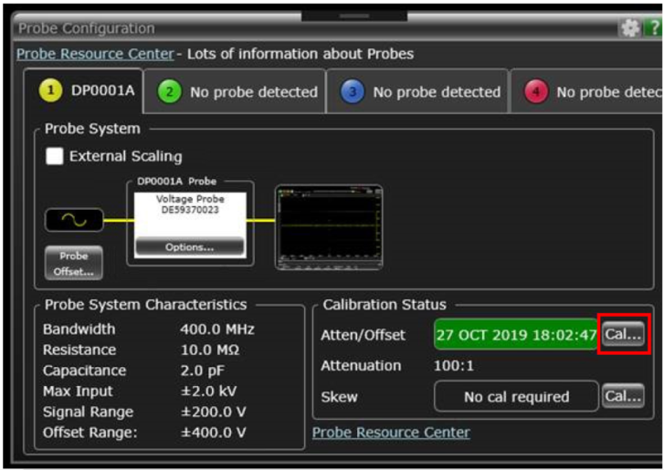
The Probe Calibration dialog box displays:
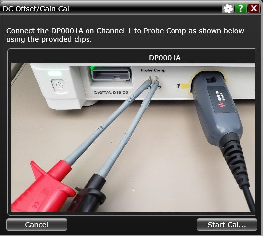
Ensure that the probe is connected to the oscilloscope as illustrated in the DC Offset/Gain Cal dialog box.
Click the Start Cal... button to initiate calibration.
Follow the instructions displayed on the Infiniium GUI screens.
DP0031A DC Offset and Gain Calibration
Not available, to be developed.
In the Compensation & Calibration section of the Control Software, software, click the Skip button when you have completed the probe compensation.
PD1550A System Calibration
Calibration requires the B2902 Precision Source/Measure Unit (SMU) and the following cables:

|
Quantity 2 required |
Black Test Patch Lead, 0.64 mm Square Pin Socket to 4 mm Stackable Banana Plug, 1 M. |
|
Quantity required |
Red Test Patch Lead, 0.64 mm Square Pin Socket to 4 mm Stackable Banana Plug, 1 M. |
Requirements
-
Perform the Oscilloscope Probe Offset Compensation first.
-
Remove the DUT module from the Interface Module before calibration.
-
Remove both High-Side and Low-Side Gate Drive modules. Depending on the calibration step, you will be instructed to re-install either the Low-Side or the High-Side Gate Drive module.
-
Install both High-Side and Low-Side Gate Drive resistor modules on the Interface module. Use a low resistance. Both resistor modules should have the same resistance value.
-
The rack and Safety Enclosure doors may be left open for calibration.
Schematic for Gate Resistor Modules
The following schematic shows the calibration terminals on the Gate Resistor modules.

2. Low-Side Gate Voltage Source Calibration -- VGS,L Output
Calibrates voltage gain and offset for the Low-Side Gate Drive.
Hardware Setup:
Remove the DUT module from the Interface Module before calibration.
Install the Low-Side Gate Drive Module on the Interface Module.
Install a low value resistance Low-Side Gate Resistance module (for example, 2.2 W).
Install UDI cables on the Low-Side Gate Drive Module and Interface Module.
Use a red calibration cable to connect the SMU red Force terminal to either of the VG pins on the Low-Side of the Interface Module.
Use a black calibration cable to connect the SMU black Force terminal to either of the KS pins on the Low-Side of the Interface Module.
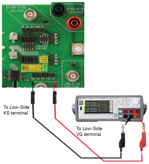
Procedure:
Click Start to perform the calibration and continue to next step.
3. Low-Side Common Resistor Calibration -- RCOM,L
Hardware Setup:
-
Remove the DUT module from the Interface Module before calibration.
-
Remove the Low-Side Gate Drive Module from the Interface Module.
-
Install the Low-Side Gate Resistor Module that you want calibrated.
-
Install a UDI cable on the Interface Module.
-
Use two sets of calibration cables for a four-wire resistance measurement as follows:
-
Red cable from SMU Force to Low-Side COM terminal.
-
Red cable from SMU Sense to Low-Side COM terminal.
-
Black cable from SMU Force to Low-Side VG terminal.
-
Black cable from SMU Sense to Low-Side VG terminal.
-
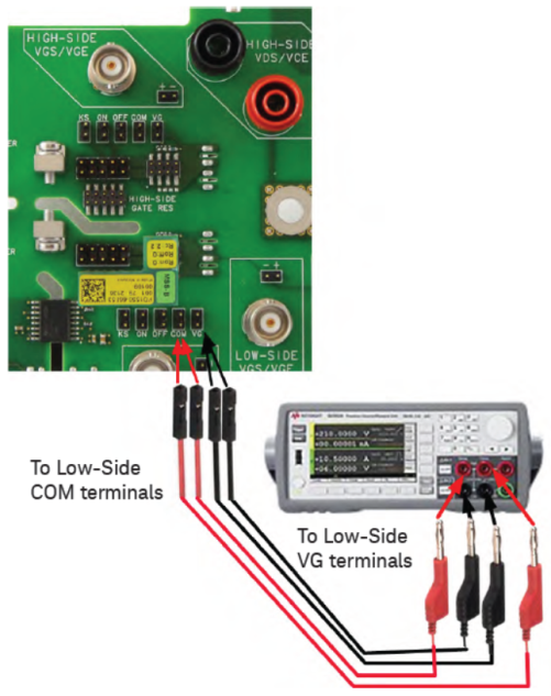
Procedure:
Click Start to perform the calibration and continue to next step.
4. Low-Side Gate Resistance Calibration -- RGON,L
Hardware Setup:
-
Remove the DUT module from the Interface Module before calibration.
-
Remove both High-Side and Low-Side Gate Drive Modules from the Interface Module.
-
Install the Low-Side Gate Resistor Module that you want calibrated.
-
Install UDI cables on the Low-Side Gate Drive Module and Interface Module.
-
Use two sets of calibration cables for a four-wire resistance measurement :
-
Red cable from SMU Force to Low-Side ON terminal.
-
Red cable from SMU Sense to Low-Side ON terminal.
-
Black cable from SMU Force to Low-Side VG terminal.
-
Black cable from SMU Sense to Low-Side VG terminal.
-
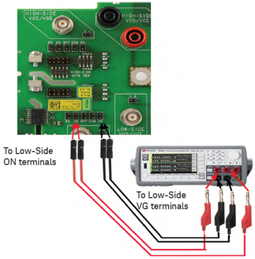
Procedure:
Click Start to perform the calibration and continue to next step.
5. Low-Side Gate Resistance Calibration -- RGOFF,L
Hardware Setup:
-
Remove the DUT module from the Interface Module before calibration.
-
Remove both High-Side and Low-Side Gate Drive Modules from the Interface Module.
-
Install the Low-Side Gate Resistor Module that you want calibrated.
-
Install UDI cables on the Low-Side Gate Drive Module and Interface Module.
-
Use two sets of calibration cables for a four-wire resistance measurement:
-
Red cable from SMU Force to Low-Side OFF terminal.
-
Red cable from SMU Sense to Low-Side OFF terminal.
-
Black cable from SMU Force to Low-Side VG terminal.
-
Black cable from SMU Sense to Low-Side VG terminal.
-
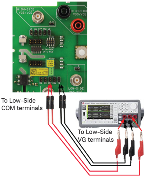
Procedure:
Click Start to perform the calibration and continue to next step.
6. High-Side Gate Voltage Source Calibration -- VGS,H Output
Calibrates voltage gain and offset for the High-Side Gate Drive.
Hardware Setup:
-
Remove the DUT module from the Interface Module before calibration.
-
Install the High-Side Gate Drive Module.
-
Install a High-Side Gate Resistance Module with a low resistance (for example, 2.2 ).
-
Install UDI cables on the Low-Side Gate Drive Module and Interface Module.
-
Use a red calibration cable to connect the SMU red Force terminal to either of the VG pins on the High-Side of the Interface Module.
-
Use a black calibration cable to connect the SMU black Force terminal to either of the KS pins on the High-Side of the Interface Module.
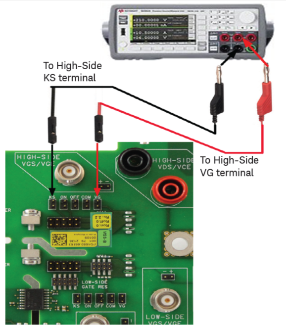
Procedure:
Click Start to perform the calibration and continue to next step.
7. High-Side Common Resistor Calibration -- RCOM,H
Hardware Setup:
-
Remove the DUT module from the Interface Module before calibration.
-
Remove the High-Side Gate Drive Module from the Interface Module.
-
Install the High-Side Gate Resistor Module that you want calibrated.
-
Install a UDI cable on the Interface Module.
-
Use two sets of calibration cables for a four-wire resistance measurement as follows:
-
Red cable from SMU Force to High-Side COM terminal.
-
Red cable from SMU Sense to High-Side COM terminal.
-
Black cable from SMU Force to High-Side VG terminal.
-
Black cable from SMU Sense to High-Side VG terminal.
-
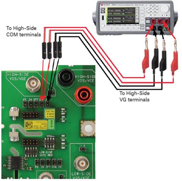
Procedure:
Click Start to perform the calibration and continue to next step.
8. High-Side Gate Resistance Calibration -- RGON,H
Hardware Setup:
-
Remove the DUT module from the Interface Module before calibration.
-
Remove both High-Side and Low-Side Gate Drive Modules from the Interface Module.
-
Install the High-Side Gate Resistor Module that you want calibrated.
-
Install UDI cables on the Low-Side Gate Drive Module and Interface Module.
-
Use two sets of calibration cables for a four-wire resistance measurement:
-
Red cable from SMU Force to High-Side ON terminal.
-
Red cable from SMU Sense to High-Side ON terminal.
-
Black cable from SMU Force to High-Side VG terminal.
-
Black cable from SMU Sense to High-Side VG terminal.
-
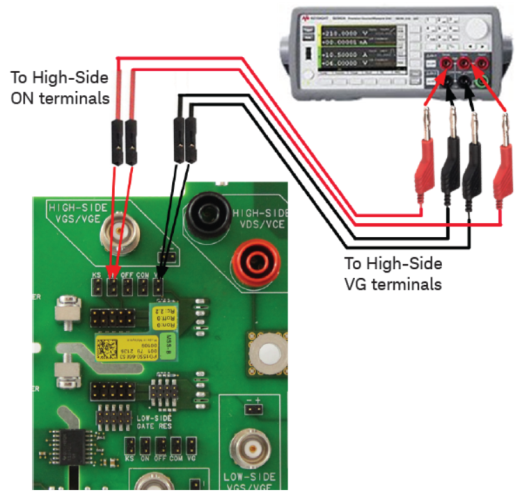
Procedure:
Click Start to perform the calibration and continue to next step.
9. High-Side Gate Resistance Calibration -- RGOFF,H
Hardware Setup:
-
Remove the DUT module from the Interface Module before calibration.
-
Remove both High-Side and Low-Side Gate Drive Modules from the Interface Module.
-
Install the High-Side Gate Resistor Module that you want calibrated.
-
Install UDI cables on the Low-Side Gate Drive Module and Interface Module.
-
Use two sets of calibration cables for a four-wire resistance measurement:
-
Red cable from SMU Force to High-Side OFF terminal.
-
Red cable from SMU Sense to High-Side OFF terminal.
-
Black cable from SMU Force to High-Side VG terminal.
-
Black cable from SMU Sense to High-Side VG terminal.
-
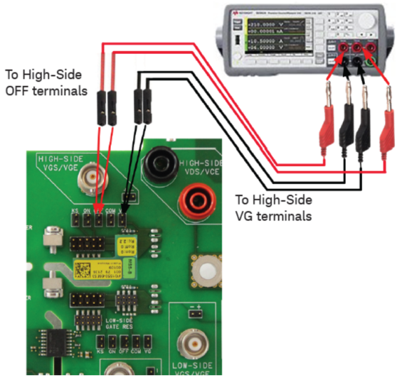
Procedure:
Click Start to perform the calibration and continue to next step.
10. Calibration Complete
Click Exit to complete the Calibration & Compensation process.
After Calibration, remove all test cables from the Interface Module and reconnect all oscilloscope probes to the Interface Module.
Coaxial Shunt Resistor Characterization
There is no separate calibration for the PD1550-61901 50 mW and the PD1550-61902 5 mW Coaxial Shunt Resistors. The De-embedding characterization file installed in the Oscilloscope provides the necessary accuracy.
This creates the latest characterization .tf2 file. After the shunt is characterized, Keysight returns the shunt to you. Download the file from the Keysight Service Portal website and install it in the oscilloscope.
Install the De-Embedding Transfer File on the Oscilloscope
-
From the temporary location where you unzipped the de-embedding file, copy the .tf2 file to the Oscilloscope. Place it in the folder:
C:\Users\ Public\Documents\Infiniium\Filters.
C:\Users\Public\Public Documents\Infiniium\Filters. However, this is an alias path. Use the path: C:\Users\Public\Documents\Infiniium\Filters in the Shunt Settings De-embedding File path in the Control Software.
-
In the PD1000A Control Software, type the .tf2 file name into the Double-Pulse Measurement Control > Settings > Instrument Configuration > De-embedding File field. For new PD1550A systems, the de-embedding file was installed in the oscilloscope at the factory with the file name:
MY5840xxxx.tf2
where xxxx is the serial number labeled on the shunt itself.